新利18全站app 中文站新利18全站app
- +86-27-87180102
-
社交媒体
 微信公众账号
 手机站
手机站 - 英文站
 微信公众账号
 手机站
手机站

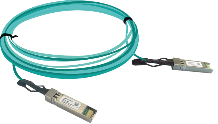
| 产品模块: | 25G SFP28 AOC |
| 订购信息: | |
| 验证码: | |
| 类 别: | 电子邮箱: | ||
| 电 话: | QQ: | ||
| *标题: | |||
| *留言内容: | |||
| *验证码: | |||
Features
lSupportData Rate 25Gbps
lBuilt-in CDR
lUp to 70m transmission distance on OM3 MMF
lUp to100m transmission distance on OM4 MMF
l850nm VCSEL and PIN receiver
lSFI electrical interface
l2-wire interface for integrated Digital Diagnostic monitoring
lSFP+MSA package with duplex LC connector
lHot pluggable
lVery low EMI and excellent ESD protection
l+3.3V power supply
lPower consumption less than 1W
lOperating case temperature: 0~+70°C
Applications
l25G BASE-SR
Compliance
lCompliant with SFF-8431
lCompliant with FC-PI-6
lRoHS compliance
Description
This product is a high data rate active optical cable (AOC), to overcome the bandwidth limitation of traditional copper cable, supporting 25.78Gbps at both electrical ends. The SFP-25G AOC assembly is a high performance integrated duplex serial data link for bi-directional communications. Physically, it is constructed out of a pair of SFP-25G terminations connected by a cable. The terminations contain the electrical connectors, the signal conditioning devices and the Physical Medium Dependent devices that are needed to ensure proper transmission across the chosen cable.
Absolute Maximum Ratings
Table1-Absolute Maximum Ratings
Parameter |
Symbol |
Min. |
Max. |
Unit |
Storage Temperature |
TS |
-40 |
+85 |
℃ |
Supply Voltage |
VCC3 |
-0.5 |
3.6 |
V |
Relative Humidity(Non-condensing) |
RH |
5 |
85 |
% |
Recommended Operating Conditions
Table2-Recommended Operating Conditions
Parameter |
Symbol |
Min. |
Typical |
Max. |
Unit |
Operating Case Temperature |
TC |
0 |
70 |
℃ |
|
Power Supply Voltage |
VCC3 |
3.13 |
3.3 |
3.47 |
V |
ICC3 |
300 |
mA |
|||
Power Dissipation |
PD |
1 |
W |
||
Data Rate |
25.78125 |
Gbps |
|||
Transmission Distance(OM3 MMF) |
70 |
m |
|||
Transmission Distance(OM4 MMF) |
100 |
m |
Optical,Electrical Characteristic
ATRS-2XXX(850nmVcseland PIN, 70m@OM3)
Tested under recommended operating conditions, unless otherwise noted
Table3-Transmitter Operating Characteristic-Optical,Electrical
Parameter |
Symbol |
Min. |
Typical |
Max. |
Unit |
Note |
Center Wavelength |
λC |
840 |
850 |
860 |
nm |
|
Laser Off Power |
Poff |
- |
- |
-30 |
dBm |
|
Average Optical Power |
Pavg |
-8.4 |
- |
2.4 |
dBm |
|
Extinction Ratio |
ER |
2 |
- |
- |
dB |
|
Differential input impedance |
100 |
Ω |
||||
Tx Input Diff Voltage |
VI |
100 |
900 |
mV |
||
Tx Fault |
VoL |
Vee |
0.8 |
V |
||
VoH |
2 |
Vcc |
V |
|||
Tx_Disable |
VIL |
Vee |
0.8 |
V |
||
VIH |
2 |
Vcc |
V |
Table4-Receiver Operating Characteristic-Optical,Electrical
Parameter |
Symbol |
Min. |
Typ. |
Max. |
Unit |
Note |
Center Wavelength |
λr |
840 |
850 |
860 |
nm |
|
Bit Error Rate |
Ber |
1E-12 |
||||
Overload |
Pin |
2.4 |
dBm |
|||
Differentialoutput impedance |
100 |
Ω |
||||
Rx Output Diff Voltage |
Vo |
400 |
800 |
mV |
||
Rx_LOS |
VoL |
Vee |
0.8 |
V |
||
VoH |
2 |
Vcc |
uA |
|||
RS0,RS1 |
VIL |
Vee |
0.8 |
V |
||
VIH |
2 |
Vcc |
V |
Table5-Control and Status I/O Timing Characteristics
Parameter |
Symbol |
Min. |
Max. |
Unit |
Note |
|
TX Disable Assert Time |
t_off |
100 |
µs |
Note1 |
||
TX Disable Negate Time |
t_on |
2 |
ms |
Note2 |
||
Time to initialize including reset of TX_Fault |
t_init |
300 |
ms |
Note3 |
||
TX Fault Assert Time |
t_fault |
1 |
ms |
Note4 |
||
Tx_Fault Reset |
t_reset |
10 |
µs |
Note5 |
||
LOS Assert Time |
t_loss_on |
100 |
µs |
Note6 |
||
LOS Deassert Time |
t_loss_off |
100 |
µs |
Note7 |
||
Serial ID Clock Rate |
f_serial_clock |
400 |
kHz |
|||
Notes:
[1] Time from rising edge of TX Disable to when the optical output falls below 10% of nominal
[2] Time from falling edge of TX Disable to when the modulated optical output rises above 90% of nominal
[3] From power on or negation of TX Fault using TX Disable
[4] Time from fault to TX fault on
[5] Time TX Disable must be held high to reset TX_fault
[6] Time from LOS state to RX LOS assert
[7] Time from non-LOS state to RX LOS deassert.
Reliability Test Definitions and Distributions
Table6-Reliability Test Definitions and Distributions
Group |
Test |
Reference |
Condition |
SS[1] |
C[2] |
Mechanical Integrity |
Mechanical shock |
MIL-STD-883E Method 2002.4 |
5 times/axis, 6 axes; 500G,1.0ms |
11 |
0 |
Vibration |
MIL-STD-883E Method 2007.3 |
Cond. A, 20G, 20-2,000 Hz, 4 min/cyc, 4cyc/axis |
11 |
0 |
|
Endurance |
Accelerated Aging |
GR-468-Core 3.3.3.1 |
85℃(Ambient Temp.) Vcc=3.3V, 2,000hrs required |
25 |
0 |
High temperature Storage |
GR-468-Core Issue 2, Section 3.4.1 |
85oC (Ambient Temp.) Vcc=3.3V, 2,000hrs required |
11 |
0 |
|
Low temperature Storage |
GR-468-Core Issue 2, Section 3.3.2.1 |
–40°C (Ambient Temp.),72hours |
11 |
0 |
|
Temperature Cycles |
MIL-STD-883C Method 1010.7 |
Non-operating, -40 oC ~ +85 oC, 10 oC /min ramp, 100 cycles pass/fail; 500 cycles for information |
11 |
0 |
|
Damp Heat |
MIL-STD-202G Method 103B |
Operating condition @ 85 oC (Ambient Temp.), /85% RH500hrs |
11 |
0 |
|
Cyclic moisture resistance |
MIL-STD-883E Method 1004.7 |
20 cycles, w/ 5 sub-cycles. |
11 |
0 |
|
Special Test |
ESD threshold |
JESD22-A114-B |
apply pulses of both polarity (+/-2000V) |
6 |
0 |
Note:
[1]SS: Sample Size;
[2]C: Maximum number of failure allowed in the test.
Pin-out Definition

Table7-Pin Assignment
Pin |
Logic |
Symbol |
Name/Description |
Note |
1 |
VeeT |
ModuleTransmitter Ground |
Note1 |
|
2 |
LVTTL-O |
TX_Fault |
ModuleTransmitterFault |
Note2 |
3 |
LVTTL-I |
TX_Disable |
Transmitter Disable;Turns off transmitter laser output |
Note3 |
4 |
LVTTL-I/O |
SDA |
2-wire Serial Interface Data Line (Same as MOD-DEF2 as defined in the INF-8074i) |
Note4 |
5 |
LVTTL-I/O |
SCL |
2-wire Serial Interface Clock (Same as MOD-DEF1 as defined in the INF-8074i) |
Note4 |
6 |
MOD_ABS |
Module Absent, connected toVeeT orVeeR in the module |
Note5 |
|
7 |
LVTTL-I |
RS0 |
||
8 |
LVTTL-O |
RX_LOS |
Receiver Loss of Signal Indication (In FC designated as RX_LOS, inSONET designated as LOS, and in Ethernet designated at Signal Detect) |
Note2 |
9 |
LVTTL-I |
RS1 |
. |
|
10 |
VeeR |
Module Receiver Ground |
Note1 |
|
11 |
VeeR |
Module Receiver Ground |
Note1 |
|
12 |
CML-O |
RD- |
Receiver Inverted Data Output |
|
13 |
CML-O |
RD+ |
Receiver Non-Inverted Data Output |
|
14 |
VeeR |
Module Receiver Ground |
Note1 |
|
15 |
VccR |
Module Receiver 3.3 V Supply |
||
16 |
VccT |
ModuleTransmitter 3.3 V Supply |
||
17 |
VeeT |
ModuleTransmitter Ground |
Note1 |
|
18 |
CML-I |
TD+ |
Transmitter Non-Inverted Data Input |
|
19 |
CML-I |
TD- |
Transmitter Inverted Data Input |
|
20 |
VeeT |
ModuleTransmitter Ground |
Note1 |
Notes:
[1]The module signal ground pins,VeeR andVeeT, shall be isolated from the module case
[2]Thispinisanopencollector/drainoutputpinandshallbepulledupwith4.7k-10kohmstoHost_Vcc onthehostboard.Pullups can be connected to multiple power supplies, however the host board design shall ensure that no module pin has voltage exceeding module VccT/R + 0.5 V.
[3]This pin is an open collector/drain input pin and shall be pulled up with 4.7k-10kohms to VccT in the module.
[4]See sff-8431 4.2 2-wire Electrical Specifications .
[5]This pin shall be pulled up with 4.7k-10kohms to Host_Vcc on the host board.
Block Diagram of Transceiver

Recommended Interface Circuit

Dimensions(All dimensions in millimeter)

Digital Diagnostic Memory Map

EEPROM Information(A0h)
Table8-EEPROM Serial ID Memory Contents (A0h)
Addr. |
Field Size |
Name of Field |
Hex |
Description |
(Bytes) |
||||
0 |
1 |
Identifer |
03 |
SFP28 |
1 |
1 |
Ext. Identifier |
04 |
SFP function is defined by serial ID only |
2 |
1 |
Connector |
0B |
Optical Pigtail |
3-10 |
8 |
Transceiver |
00 00 00 00 00 08 00 00 |
SFP28 Cable Technology: Active Cable |
11 |
1 |
Encoding |
03 |
NRZ |
12 |
1 |
BR, Nominal |
FF |
>25Gb/s |
13 |
1 |
Rate Identifier |
00 |
Unspecified |
14 |
1 |
Length (9um) km |
00 |
|
15 |
1 |
Length (9um) 100m |
00 |
|
16 |
1 |
Length (50um)10m |
00 |
|
17 |
1 |
Length (62.5um) 10m |
00 |
|
18 |
1 |
Length (Copper or OM4) |
03 |
线缆长度为(03,05,07,10m) |
19 |
1 |
Length (50um OM3) |
00 |
|
20-35 |
16 |
Vendor name |
48 47 20 47 45 4E 55 49 4E 45 20 20 20 20 20 20 |
“HG GENUINE” Vendor Name(ASCII) |
36 |
1 |
Transceiver |
18 |
25GAUI C2M AOC,BER<10^(-12) |
37-39 |
3 |
Vendor OUI |
00 00 00 |
Unspecified |
40-55 |
16 |
Vendor PN |
41 54 52 53 2D 32 30 30 33 20 20 20 20 20 20 20 |
“ATRS-2003”Part No.(ASCII) |
56-59 |
4 |
Vendor rev |
31 2E 30 20 |
“1.0”(ASCII) |
60-61 |
2 |
Wavelength |
00 00 |
Transceiver wavelength |
62 |
1 |
Reserved |
00 |
|
63 |
1 |
CC_BASE |
CS |
Check code for Base ID Fields |
64-65 |
2 |
Options |
08 3A |
a conventional uncooled laser Power Level 1a conventional limiting outputthe transceiver has an internalretimer or CDR,RATE_SELECT,TX_DISABLE,TX_FAULT,Rx_LOS |
66 |
1 |
BR,MAX |
67 |
Unspecified |
67 |
1 |
BR,MIN |
00 |
Unspecified |
68-83 |
16 |
Vendor SN |
43 53 31 36 34 33 38 38 38 30 30 37 35 20 20 20 |
Serial Number of transceiver(ASCII). |
84-91 |
8 |
Date code |
31 36 31 31 30 31 20 20 |
Manufactory Date Code. |
92 |
1 |
DiagnosticMonitoring Type |
60 |
Digitaldiagnostic monitoringimplemented,“Internallycalibrated”is implemented OMA |
93 |
1 |
Enhanced Options |
FA |
soft Rate Select,Alarm/warning flags,soft TX_DISABLE,soft TX_FAULT,soft RX_LOS,soft RATE_SELECT |
94 |
1 |
SFF_8472Compliance |
08 |
Includes functionality described in Rev12.0 SFF-8472 |
95 |
1 |
CC_EXT |
Cs |
Check sum for Extended ID Field. |
96-127 |
32 |
Vendor Specific |
Read only |
Depends on customer information Filled by zero |
Regulatory Compliance
Table9-Regulatory Compliance
Feature |
Reference |
Performance |
|
Electrostaticdischarge(ESD) |
IEC/EN 61000-4-2 |
Compatible with standards |
|
Electromagnetic Interference (EMI) |
FCC Part 15 Class B EN 55022 Class B (CISPR 22A) |
Compatible with standards |
|
Laser Eye Safety |
FDA 21CFR 1040.10, 1040.11 IEC/EN 60825-1,2 |
Class 1 laser product |
|
Component Recognition |
IEC/EN 60950,UL |
Compatible with standards |
|
ROHS |
2002/95/EC |
Compatible with standards |
|
EMC |
EN61000-3 |
Compatible with standards |
|
Safety regulation requirement |
UL |
UL60950-1 |
Compatible with standards |
TUV |
IEC/EN60950-1,IEC/EN60825-1,IEC/EN60825-2; |
Compatible with standards |
|
VDE |
IEC/EN60950-1,IEC/EN60825-1,IEC/EN60825-2; |
Compatible with standards |
|
FDA |
21 CFR 1040.10 & 1040.11 |
Compatible with standards |
|
Ordering Information
Table10-Ordering Information
Part No. |
Specification |
Application |
||||||||
Pack |
Rate |
Tx |
Pout |
Rx |
S |
Top |
Reach |
Others |
||
ATRS-2001 |
SFP28 |
25G |
850nm Vcsel |
\ |
PIN |
\ |
0~70℃ |
1m |
DDM/RoHS |
25G Base-SR |
ATRS-2003 |
SFP28 |
25G |
850nm Vcsel |
\ |
PIN |
\ |
0~70℃ |
3m |
DDM/RoHS |
25G Base-SR |
ATRS-2005 |
SFP28 |
25G |
850nm Vcsel |
\ |
PIN |
\ |
0~70℃ |
5m |
DDM/RoHS |
25G Base-SR |
ATRS-2007 |
SFP28 |
25G |
850nm Vcsel |
\ |
PIN |
\ |
0~70℃ |
7m |
DDM/RoHS |
25G Base-SR |
ATRS-2010 |
SFP28 |
25G |
850nm Vcsel |
\ |
PIN |
\ |
0~70℃ |
10m |
DDM/RoHS |
25G Base-SR |
ATRS-2020 |
SFP28 |
25G |
850nm Vcsel |
\ |
PIN |
\ |
0~70℃ |
20m |
DDM/RoHS |
25G Base-SR |
